In the last post, we studied the hybrid-pi model of E-MOSFET, in this post we are going to see Ac-Analysis of MOSFET or in short designing an amplifier with E-MOSFET.
We know that with the help of Dc-Analysis we find certain parameters which are very important while designing any amplifier and those parameters are transconductance(gm), output current(Id), and Vth. So now we will focus on the ac-analysis of MOSFET to find certain ac parameters which are required to design any amplifier.
@ AC-ANALYSIS OF E-MOSFET:-
As you can see in the above diagram all the capacitors shown in the circuit will be shorted because capacitors act as a short circuit for the ac-signal.
So the ac model of the E-MOSFET would look as shown below.
As we had studied the ac-analysis of the BJT, there we had seen 4 important parameters and they were
1) Current Gain (Ai)
2) Input Resistance (Rin)
3) Output Resistance (Rout)
4) Output Voltage (Vout)
1) Current Gain:-
As we all know the MOSFET is a voltage-controlled current source. Therefore for the ac-analysis of MOSFET, this parameter is absent as the input current is zero or almost negligible.
2) Input Resistance:-
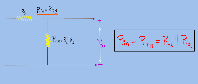
As you can see the dc source is grounded since we are dealing with the ac-analysis therefore R1 and R2 will be in parallel with each other. Thus the resultant resistor will be Rth = R1 || R2. Also, we can clearly see that Rs is in series with the Rth.
But Rs won't be included in the internal resistance of the amplifier as it is the internal resistance of the AC voltage source.
3) Output Resistance:-
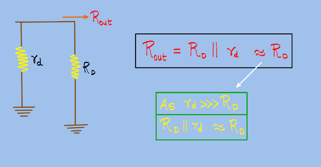
In the above diagram, you can clearly see that the resistance rd of the MOSFET is parallel to drain resistance Rd. Therefore the output resistance of an amplifier is equivalent to - Rout = RD || rd.
Now rd>>>RD
Thus Rout = RD
4) Voltage Gain:-
Now since we had completed BJT Amplifier and there we had seen the formula for voltage gain.
Voltage Gain = Av = Vout / Vin
So we need to find out the input voltage and output voltage of the amplifier separately and in the end, substitute them in the above equation.
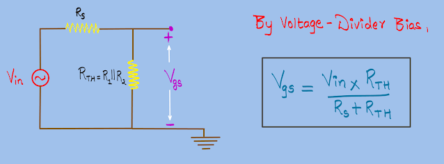
As you can see in the above figure, by applying voltage divider bias we had calculated the gate to source voltage Vgs.
Vgs = Vin*Rth / Rs+Rth .......(1)
Now analyzing the output side, as you can see over here gmVgs is moving in the opposite direction to Vout. Therefore by applying KVL to the output loop we get the above equation. In which we substitute the value of Vgs from equation (1). Then we move Vin to the LHS side which comes in the denominator to Vout.
Thus Av = Vout / Vin = - (gm*Rth*RD||rd) / (Rs + Rth)
Negative sign indicates that there is 180 degree phase shift between the input and the output signal.


With a keen eye on breakthroughs and global tech trends, DiscoverTechInfo is an invaluable resource for anyone passionate about technology. Their detailed reporting and thoughtful analysis inspire learning, curiosity, and a deeper understanding of digital innovation.
ReplyDeleteI value NewsWordPage for its thoughtful journalism and clear presentation. Each article explains complex topics in politics and technology while maintaining accuracy, ensuring readers can follow developments confidently and gain a deeper perspective on today’s global issues.
ReplyDeletePractical-buddy moments capture creativity, learning, and everyday inspiration through hearthstats net news , creating visually engaging content. Each shot highlights useful ideas and thoughtful expression in a simple and artistic way.
ReplyDelete